My Joomla
Manufacturer of laser solutions

Marking, laser engraving

Marking, laser engraving

Laser marking and engraving Laser marking or engraving are processes that have been widely used in industry for several decades for identification or traceability purposes. It constitutes an advantageous industrial alternative to many mechanical, thermal or inking processes on many materials, metals, plastics or organic. Laser marking, without contact with the part to be marked, and able to reproduce with finesse and aesthetically complex shapes (texts, logos, photos, bar codes or 2D codes) offers great flexibility of use and does not require any consumable.

The materials

Almost any material can be marked with a laser source. As long as you use the correct wavelength. Infrared (IR) is most commonly used (1.06 microns and 10.6 microns) on most materials. Laser markers with wavelengths in the visible or ultra violet have also been used. On metals, whether by etching or surface annealing, it provides durability and resistance to acids and corrosion.

On plastics, the laser acts by foaming, or by coloring material in addition to pigments possibly present in it.

Marking on transparent materials is also possible with lasers of the appropriate wavelength, usually UV or CO2.

On organic materials, laser marking generally acts thermally. We will also use a laser marker on all these materials for a marking by ablation of a layer or a surface treatment of the part to be marked.

.

Semiconductor wafer marking

The applications of traceability marking on wafers mainly consist of 2 distinct processes: the so-called "DeepMark" marking by vaporization of material, down to depths of 150 µm, and the "SoftMark" marking on polished edges, without emission of particles, for depths from 0.1 to 4µm. All types of markings used in SEMI (OCR, T7 data matrix, 2D cell code, BC412, etc.) are supported by our systems. A wide range of laser sources (IR, 532nm, UV or CO2) make it possible to address all materials and surfaces currently used in the field of semiconductors. Dot diameters are fixed or programmable over a range of 50 to 110µm, for wafer thicknesses.

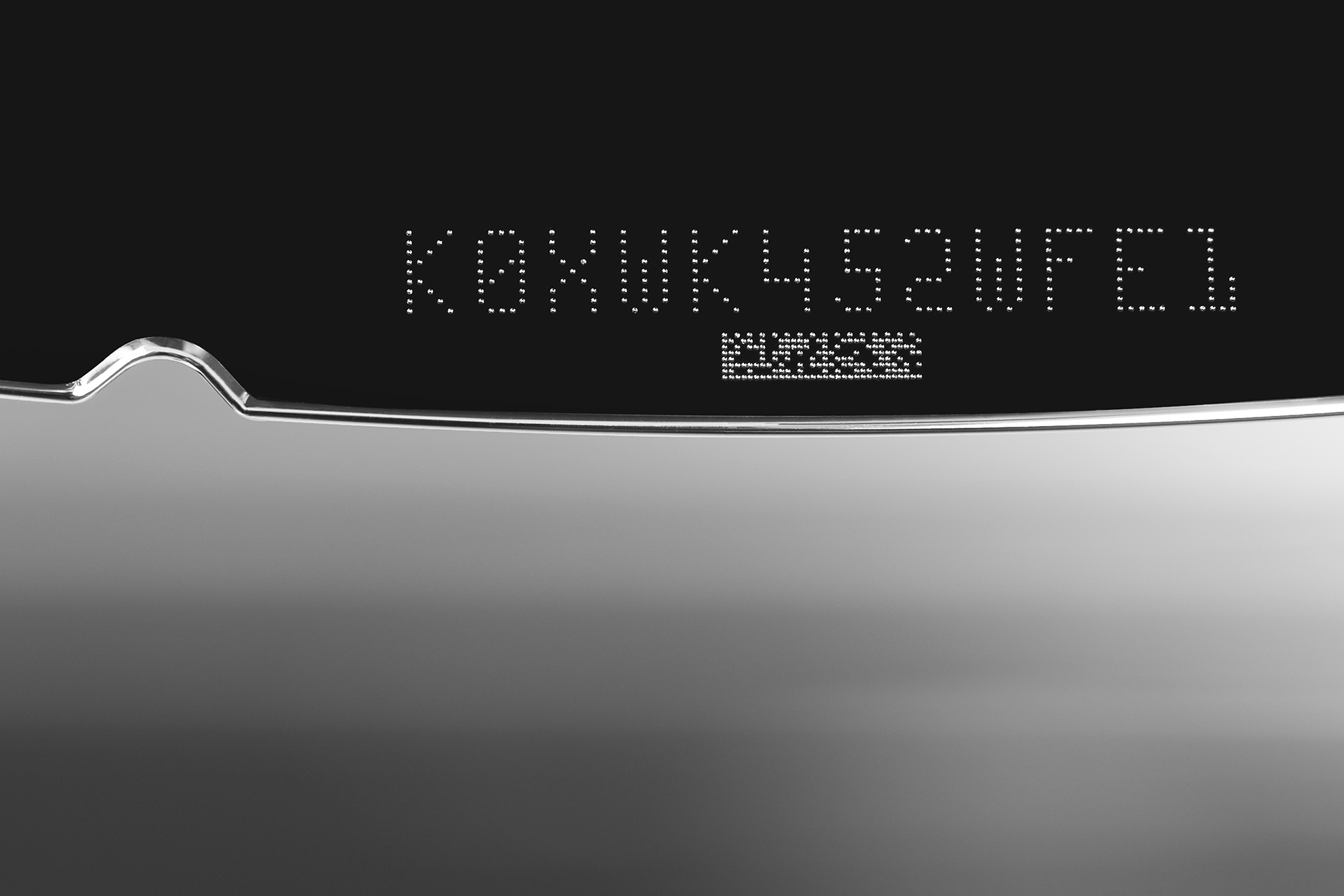
Example of laser marking on a silicon wafer

.

Marking and texturing on different types of parts and materials.

Examples of laser markings made with FOBA laser markers

Marquage laser sur plastique
Marquage laser sur fonte
Marquage laser sur Inox
Marquage laser par ablation par laser
Marquage laser par moussage
Texturation par gravure laser

Save
Cookies user preferences
We use cookies to ensure you to get the best experience on our website. If you decline the use of cookies, this website may not function as expected.
Accept all
Decline all
Read more
Analytics
Tools used to analyze the data to measure the effectiveness of a website and to understand how it works.
Google Analytics
Accept
Decline
Functional
Tools used to give you more features when navigating on the website, this can include social sharing.
Joomla!
Accept
Decline